IBM Thomas J. Watson Research Center
Ossining, New York
“For more than sixty years, IBM Research has been the innovation engine of the IBM corporation. From helping the Apollo space missions land on the moon to the discovery of fractals; from the technology behind laser eye surgery to a question answering computer called Watson now being applied to health care, IBM Research continues to define the future of technology.”
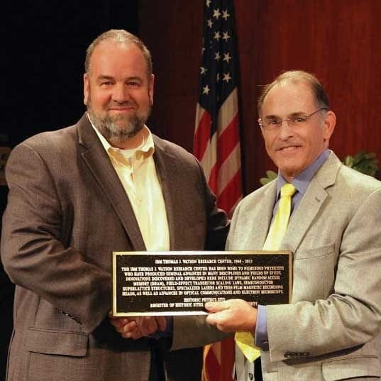
And at its research heart is the Thomas J. Watson Research Center in Yorktown Heights, New York, which serves as the headquarters for IBM Research, the largest industrial research organizations on the planet. The Center has produced myriad advances in physics, as well as many other related fields. It is known as a driver of technical revolution and as such, on 5 December 2013, APS vice-President Sam Aronson presented a plaque to IBM Research vice-President of Technical Strategy and Worldwide Operations David McQueeney, as part of the APS Historic Sites Initiative. The citation reads: “The IBM Thomas J. Watson Research Center has been home to numerous physicists who have produced seminal advances in many disciplines and fields of study. Innovations discovered and developed here include dynamic random access memory (DRAM), field effect transistor scaling laws, semiconductor superlattice structures, specialized lasers and thin-film magnetic recording heads, as well as advances in optical communications and electron microscopy.”
The T. J. Watson Research Center was designed by preeminent architect Eero Saarinen and completed in 1961, and has been home to such notable figures as physicists Charles H. Bennett, Nobel Laureate Leo Esaki, Richard Garwin and Rolf Landauer, as well as mathematician Benoît Mandelbrot and electrical engineer Robert Dennard. The large curving hallway running along the building serves as a promenade in which IBM scientists and engineers converse and hold discussions at specifically designed alcoves that face out to the forest that lies beyond. IBM physicists have won multiple APS Prizes and Awards, including the Aneesur Rahman Prize for Computational Physics, the Dannie Heineman Prize for Mathematical Physics, the Davisson-Germer Prize in Atomic or Surface Physics, the George E. Pake Prize, the Irving Langmuir Prize in Chemical Physics, the James C. McGroddy Prize for New Materials, the Max Delbruck Prize in Biological Physics, the Oliver E. Buckley Condensed. In 2009, the Watson Research Center was declared an IEEE Milestone in Electrical Engineering and Computing for research conducted in its first 25 years.
The Center’s significant role in the history of physics research cannot be denied. IBM scientists first produced lasers here, using calcium fluoride crystals doped with two different ions, and today these are universally recognized as being among the earliest laser systems. Semiconducting device innovations include one of the first demonstrations of a semiconductor-based injection laser, dynamic random access memory (DRAM), semiconducting quantum well and superlattice structures, and field effect transistor (FET) scaling laws. Other innovations include amorphous magnetic films for optical storage technology and thin-film magnetic recording heads.
The invention of the one-transistor DRAM became the industry standard for random access memory (RAM) and enabled the microcomputer revolution. Semiconductor quantum wells and injection lasers have revolutionized telecommunications and have enabled devices like the compact disk. FET scaling laws involve reducing the dimensions of metal-oxide field effect transistors (MOSFETs) and their interconnecting wires, leading to simultaneous improvements in transistor density, switching speed, and power dissipation. The scaling theory has driven miniaturization in the semiconductor industry by providing the industry a roadmap for setting targets and expectations for generations of process technology. This roadmap has enabled portable computing, from laptops to cell phones.
Researchers at T. J. Watson have also been responsible for major innovations in silicon microprocessor technology over the past 40 years. These have included copper interconnect technology, which replaced aluminum wiring in chips, devices based on silicon-germanium, and, more recently, integrated circuits that employ high dielectric constant oxide and metal gate technology, in which the materials used to make a silicon transistor were revamped in order to enable continued transistor scaling.
Innovations in thin-film fabrication processes facilitated the realization of inductive and magnetoresistive thin-film heads for large-scale magnetic storage. Since the introduction of IBM’s first magnetic disk storage system in 1956, the density of storage and speed of access has continuously improved. A quantum jump in the rate of improvement was enabled by the invention of thin film, read/write magnetic recording heads. Without this capability to quickly access an enormous amount of data on magnetic disk drives, many technologies we now take for granted, such as the Internet, would not exist.
Today IBM research is comprised of 12 labs around the world with approximately 3,000 research scientists working on creating adventures in technologies varying from quantum computing to new cognitive learning systems based on the breakthroughs established by The IBM Watson question answering system.